Intel’s Xe for HPC: Ponte Vecchio with Chiplets, EMIB, and Foveros on 7nm, Coming 2021
by Dr. Ian Cutress on November 17, 2019 7:00 PM EST
Today is Intel’s pre-SC19 HPC Devcon event, and with Raja Koduri on stage, the company has given a small glimpse into its high-performance compute accelerator strategy for 2021. Intel disclosed that its new hardware has the codename ‘Ponte Vecchio’ and will be built on a 7nm process, as well as some other small interesting bits.
Ever since Intel hired Raja Koduri from AMD’s Graphics division, the ambition in which Intel has been assembling its discrete GPU push has made for a strong injection of competition into this industry. Today a modern graphics architecture needs to be many things to many people: low powered for small chips, high performance for gaming and VR, perform sizable compute for HPC, and detail with different types of convolution and matrix math as AI becomes more important. Intel has already disclosed that its future products will bear its new ‘Xe’ architecture (that’s a superscript e), and that they plan to cover the spectrum all the way from integrated graphics to high performance computing, but that’s about all we have been told.
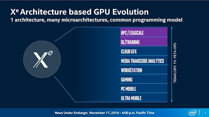
As part of the keynote speech today, Koduri has explained that Intel will have a single ‘Xe’ architecture but multiple sub-architectures / microarchitectures (or however you want to characterize it in a GPU) in order to address different parts of the market. The ultra-mobile parts of the product stack might focus on small die size and high efficiency libraries, whereas a compute product might have high double-precision performance and run high-performance libraries. Some variants might have the equivalent of tensor accelerators for AI, or some variants might have bigger cache variants to manage specific customer needs. Rather than a ‘one size fits all’ approach, it appears that Intel are going to stretch Xe as wide as they need to in order to accommodate as many customers as possible.
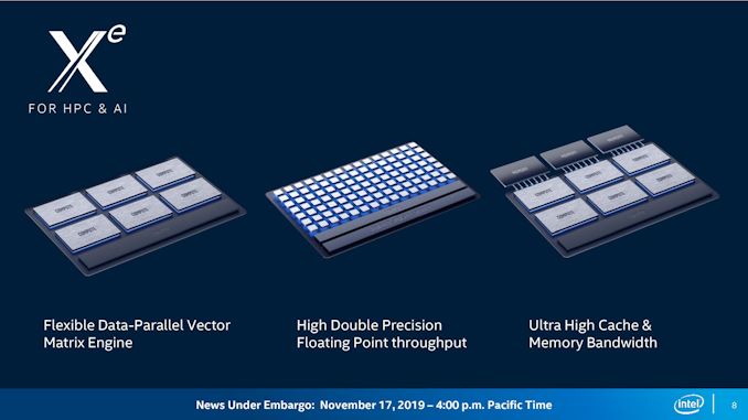
For high-performance computing, the presentation highlighted three key areas that the Xe architecture will be targeting. First is a flexible data-parallel vector matrix engine, which plays into the hands of AI acceleration and AI training in a big way. The second is high double precision (FP64) throughput, which has somewhat been disappearing of late due to reduced precision AI workloads, but is still a strong requirement in traditional HPC workloads like, weather, oil and gas, and astronomy. (We should point out that the diagram shows a 15x7 block of units, and Intel’s Gen architecture uses 7 threads per execution unit.) The third tine in this trident is that Intel’s HPC efforts will have a high cache and memory bandwidth, which the slides suggest will be directly coupled to individual compute chiplets ensuring a fast interconnect.
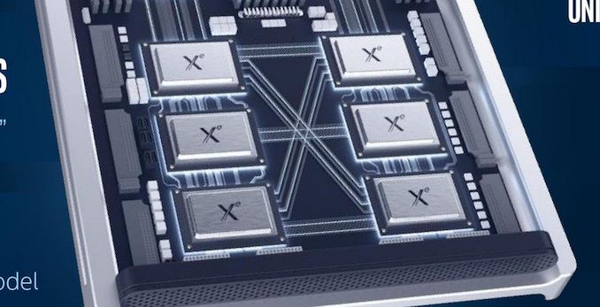
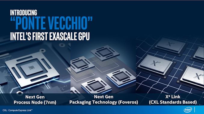
So in this case, enter Ponte Vecchio, named after the bridge that crosses the river Arno in Florence, Italy. This will be Intel’s first ‘exascale class’ graphics solution, and is clearly using both chiplet technology (based on 7nm) and Foveros/die stacking packaging methods. We further confirmed after our call, based on discussions we had with Intel earlier in the year, that Ponte Vecchio will also use Intel’s Embedded Multi-Die Interconnect Bridge (EMIB) technology, joining chiplets together. Pulling all the chips into a single package is fine, meanwhile GPU-to-GPU communication will occur through a Compute eXpress Link (CXL) interface, layered on top of PCIe 5.0.
So while this is an important development in the disclosure of Intel’s graphics strategy, specifically speaking to the HPC crowd, it still leaves a lot of questions to be answered: what exactly is Xe, how is compute handled differently from shaders, how has Intel solved the chiplet paradigm in GPUs (latency and bandwidth needs), how many chiplets per GPU, power consumption targets, what is stacked with Foveros, how is the memory connected, what type of memory, what are the performance targets, how many chiplets, what size of the chiplets, what exactly is 7nm, and so forth. What we do know at this point is that Intel is using a vector matrix engine, offers high FP64 performance, high memory bandwidth, and that for Intel, this is their ‘first exascale GPU’. In short, we're still in the early days of the Xe story, at least from a public perspective.
It’s worth noting that earlier this year, we were invited to discuss the future of Intel packaging with Ramune Nagisetty, who stated that technologies such as chiplets, Foveros (die stacking), and Intel’s Embedded Multi-Die Interconnect Bridge (EMIB) are all going to play critical roles in the future of Intel’s products, and specifically for the use the upcoming graphics portfolio. Part of that discussion was officially off the record, until today, such as the Ponte Vecchio code name. Ponte Vecchio (PV for short) is just one part of Intel’s Xe plans, as we have already been promised GPUs on 10nm.
Ponte Vecchio will be the showcase accelerator in the Aurora supercomputer, to be installed at Argonne National Laboratory in 2021. Intel has announced that this will feature two Sapphire Rapids CPUs (the one after Ice Lake), along with six Ponte Vecchio GPUs, in a single node. More details on this in our Aurora coverage.
Related Reading
- Intel's Interconnected Future: Combining Chiplets, EMIB, and Foveros
- Intel to Support Hardware Ray Tracing Acceleration on Data Center Xe GPUs
- Intel’s Xeon & Xe Compute Accelerators to Power Aurora Exascale Supercomputer
- Intel Details Manufacturing through 2023: 7nm, 7+, 7++, with Next Gen Packaging


16 Comments
View All Comments
firewrath9 - Sunday, November 17, 2019 - link
Hopefully Intel makes good drivers. Perhaps with intel's massive budget they could make a competitor to CUDA, perhaps it can even be open source. Long shot though.Yojimbo - Monday, November 18, 2019 - link
I don't think it matters if it is open source or not. There are plenty of cross-compilers for CUDA code. The issue is that you can't just make a compiler that takes CUDA code optimized for NVIDIA's hardware that then optimizes it for some other hardware and expect that code to run well. You still have to rewrite a lot of the code to fit the other architecture, and CUDA wasn't designed to support other architectures. Now, if Intel did make their API open source, they still aren't going to be adding support to it for rival architectures, and it will still take hand optimization to effectively target those other architectures if they or someone else did, so the issue is much the same.There was the same issue with Xeon Phi. Intel promised that you could take existing x86 code and just compile it on a Xeon Phi. That was true, but it ran horribly without hand optimization that took about as much effort as it took to get something to run well on a GPU. What has to be understood is that these accelerated portions of the code are a small portion of the total code base but they take up the vast majority of executed operations. For acceleration to be effective it should be optimized carefully. Now very large and legacy code bases, such as exist in the academic world, would take a lot of effort to parallelize using CUDA or OpenCL, etc., and they get a good amount but not all of the benefit by using compiler directives through OpenMP or OpenACC. But that is neither here nor there as far as CUDA or Intel's forthcoming GPU API are concerned, because they are already fully portable on NVIDIA or anyone else's hardware to any hardware that has a compiler written for it. It's orders of magnitude less work to write such a compiler and focus some work on core math libraries used by the compiler than to implement anything in to-the-metal APIs like CUDA. For the foreseeable future, I would bet almost all code run on Intel and AMD's compute GPUs will be 1) run through OpenACC and OpenMP compiler directives and not using a low level API or 2) be focused on certain narrow use cases, mainly deep learning frameworks like TensorFlow. NVIDIA have spent billions of dollars over years to develop their trove of CUDA libraries, all optimized for their architecture. It will take years for Intel to have a chance to catch up, and AMD probably doesn't have the money to do so.
OpenCL takes the opposite approach as CUDA and presumably the way Intel's API will be approached. It implements things in the language by committee which then should be implemented into the architectures. I guess if you are lucky you can get the things you are working on in your architecture implemented into OpenCL, but it's still going to come along a lot more slowly than if you are able to implement it in your own language yourself. GPU architectures are currently changing so quickly at the moment that the OpenCL approach is backwards. There's no way OpenCL can keep up.
Amandtec - Monday, November 18, 2019 - link
The only possible way to beat Cuda (Nvidea) now is if MS, Intel, Google and everyone else pool their resources together and heavily outspent Nvidia for a few years to develop something much better thus warranting a code rewrite. Of course, they won't - and so will repeat the lesson Intel learned with mobile and Microsoft learned with Windows mobile : being late to market is the same as having an inferior product - because standards and ecosystems (i.e. the software) has all already been built now and people will not easily rebuild it.Yojimbo - Monday, November 18, 2019 - link
I mostly agree but there are some particulars to the current situation that mean there's a chance:1) The basic architecture that serves the bulk of the lucrative and growing data center market also can serve the gaming, graphics, and HPC markets. These markets can be served without a thriving compute API, and so there is the opportunity for the architecture to hang around for years and slowly build software support for the data center market. In addition, Intel is in a very good position to break into those other markets as long as they can make good products, owing to their client CPU and data center businesses. The Atom architecture and the Windows Mobile operating system were specialized endeavors with much less value if they didn't succeed in those single domains (although, Intel also tried to use Atom in the Xeon Phi, which also failed).
2) AI is a possible entry point to the data center that potentially, depending on how it ends up being used, may require relatively little software support in order to address a sizable revenue stream.
So Intel is fighting an uphill battle, but there are reasons they may hope that if they execute well and by using their large resource pool and huge market power they may be able to break into the segment even at this late date. Of course, what they should have done was to pursue a GPU years ago instead of fooling around with Xeon Phi. My personal gut feeling is that this OneAPI thing will end up being as much marketing gobbledygook as Intel's promise of using Xeon Phi to effectively accelerate existing x86 code. It doesn't matter if you're using "OneAPI" if you have to refactor your code to effectively target the different architectures, anyway.
Yojimbo - Monday, November 18, 2019 - link
To follow on the OneAPI thing: yes, you can, for example, plug in a different function from a different library that has a common interface, one that targets a GPU and one that targets a CPU or an FPGA or the NNP. But the problem is that different algorithms are suited better to different architectures. Targeting a CPU you may ideally want to tackle the problem entirely differently at the algorithmic level compared with targeting a GPU.JayNor - Saturday, December 7, 2019 - link
Their oneAPI dpc++ uses Sycl along with Intel's extensions.https://spec.oneapi.com/oneAPI/Elements/dpcpp/dpcp...
edzieba - Tuesday, November 19, 2019 - link
It's not development they need to compete on with Nvidia, it's developer support. If you're using CUDA (or for that matter, the consumer-side graphics drivers or Gameworks), Nvidia will bend over backwards to help you implement and optimise it. With OpenCV? AMD will happily point you to the source code, and if you ask very nicely read you the documentation.JayNor - Sunday, November 24, 2019 - link
The oneAPI OSPRay is already compatible with AMD CPUs.https://www.phoronix.com/scan.php?page=article&...
What is not clear is whether the new GPU support will be easily ported.
"I’m pleased to share today that the Intel® Xe architecture roadmap for data center optimized rendering includes ray tracing hardware acceleration support for the Intel® Rendering Framework family of API’s and libraries."
https://itpeernetwork.intel.com/intel-rendering-fr...
JayNor - Sunday, November 24, 2019 - link
The intel dpc++ is built on top of SYCL, according to the announcements. The SYCL implementation shows use of a SYCL for OpenCL variant that apparently is a common interface to OpenCL implementations on FPGA, DSP, GPU and CPUs, according to their diagram. Perhaps this is the direction of Intel OneAPI. In that case, the portability to NVDA and AMD GPUs would depend on how well this SYCL for OpenCL handles the different OpenCL targets.https://www.khronos.org/sycl/
"Codeplay, which is already known for their several Vulkan / SYCL / SPIR-V initiatives, is working on this layer to run oneAPI / DPC++ / SYCL codes atop NVIDIA hardware while still leveraging NVIDIA's CUDA drivers."
https://www.phoronix.com/scan.php?page=news_item&a...
Dragonstongue - Monday, November 18, 2019 - link
with how many hands Intel has in everyones cookie jar it would not surprise me in the least it either fall flat on it's face OR has immensely potent day of release support (forcing "partners" to make sure of it or they lose support from Intel outright with "sweetheart deals"